Hello,
I am attempting to build my own nitrokey. I have the LPC part as a HTQFP64 package instead of BGA98. I understand that this will require some adjustments within the firmware with gpio referencing/assignment, and also definitely adjustments rerouting pins, tracks, connections on the pcb and schematic. that’s ok for me, I learn along the way. I don’t want to inconveniece someone else if its difficult or annoying, but hopefully its a straight forward process. Only a few things concern me so far, I think i can do it. I’m using kicad 8.
some references:
lpc datasheet: https://www.nxp.com/docs/en/data-sheet/LPC55S6x.pdf
nitrokey3c hardware git: GitHub - Nitrokey/nitrokey-3c-nfc-lpc55-hardware: Nitrokey 3 USB-C NFC LPC55 hardware
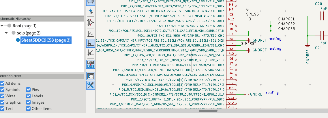
i’ve attached some images of my progress so far. ( apparently new users can only upload one image. I picked what I thought was most relevant.
some confusion/questions.
- The schematic shows CHARGE1, CHARGE2, CHARGE3 on Pad C7. The CHARGE1 input is the only one without the no connect flag. On the PCB, it’s Pad C7 that should be connected to this, but C7 doesn’t appear to be connected to anything. Is that correct, or am I overlooking something? What is the purpose of these CHARGE assignments?
Thats all for now, I hope to add more questions as I move along. For now I will continue, I will try and properly re-assign the RGB placments onto different gpio pins because the HTQFP Package has less GPIO pins to work with.
Thank you for reading.